PCB Designing
Convert your schematic into a physical Printed Circuit Board (PCB) and prepare for manufacturing.
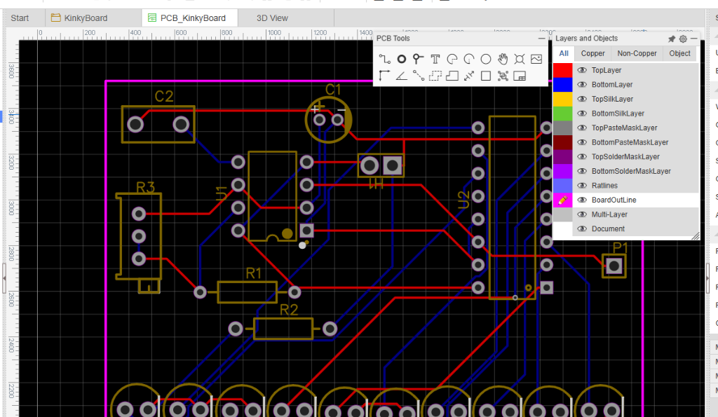
Convert Schematic to PCB
At the top of your screen in EasyEDA, click Design > Convert Schematic to PCB.
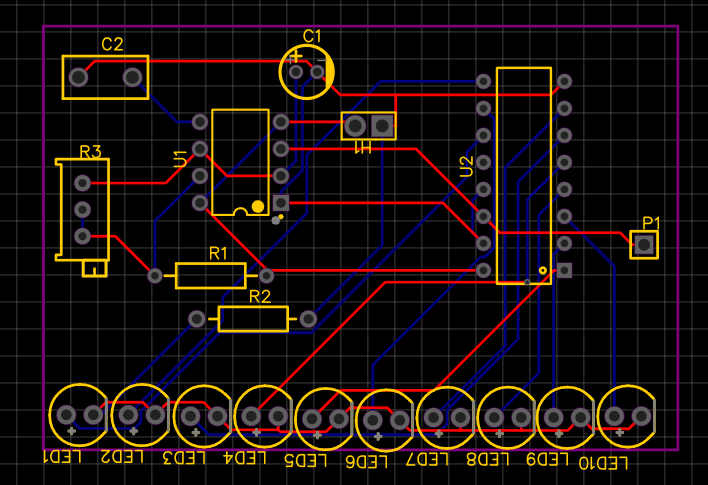
If you see a warning about nets, click "Check Net" or just proceed. Now, you should see your components inside a purple rectangle.
Create a Custom Outline
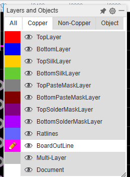
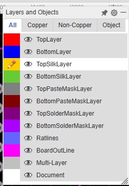
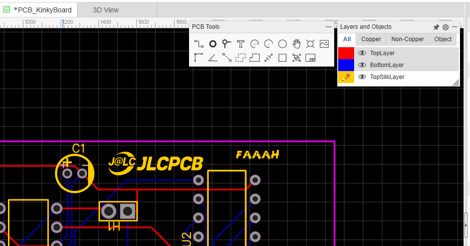
The purple lines are your BoardOutLine. You should customize this! A custom shape makes your board unique.
- Select the BoardOutLine layer in the sidebar (highlighted in pink/purple).
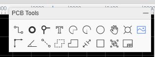
- Use the Track tool to draw your shape.
- Keep your board size below 100x100mm.
Routing your Traces
The blue ratlines show you the connections but they aren't real wires yet. You need to "route" them with copper tracks.
- Select the TopLayer (Red) or BottomLayer (Blue).
- Click 'W' or the Track tool to draw copper lines between pads.
- If wires must cross each other, click 'V' to place a Via and switch to the other side of the board.
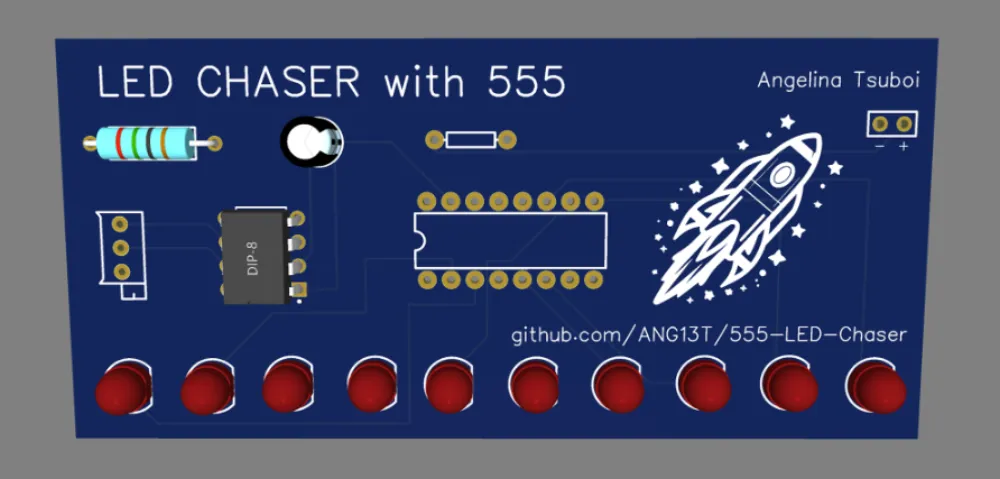
Add Custom Art
You can add text and images to your board using the TopSilkLayer (the white ink).
IMPORTANT: You must add the JLCPCB logo to your silkscreen to show your support! You can find it in the EasyEDA library or import it as an image.
Go to File > Import > Image to add your own logo or artwork to the board.
Manufacturing Files
Once you pass the Design Rules Check (Design > DRC), it's time to export. You need a "Gerber" file.
- Click File > Generate PCB Fabrication File (Gerber).
- Click "No, Generate Gerber Anyway" if prompted.
- Download the zip file.
JLCPCB Ordering
Go to jlcpcb.com and upload your Gerber zip file. You should see an instant quote!
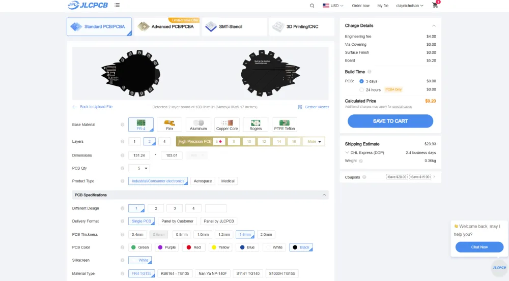
- Layers: 2
- Materials: FR-4
- PCBA: NO (We will hand-solder these!).
Once you have your price, take a screenshot of the quote with Global Standard Direct shipping selected.